

Principle and Application of Linear Regulator LDO

2021/08/30
introduction
DC/DC converters have been widely used in various mobile electronic systems, such as mobile communication terminals, portable computers, PDAs, etc. Low-voltage, low-dropout (Low Dropout) linear regulator LDO is functionally a step-down transformer in DC/DC converters, with simple structure, low noise, low power consumption, small package and less peripheral application devices, etc. With outstanding advantages, it has been widely used in portable electronic products.
Overview of LDOs
LDO (Low Dropout) linear regulators have higher power conversion efficiency than traditional regulators, and have simpler structure, lower cost and lower noise characteristics than switching regulators, so it increasingly popular in portable electronics. LDO linear regulators and switching regulators are the two most commonly used power management circuits in portable electronics today.
There are two types of LDOs, Bipolar (bipolar) and CMOS (unipolar). In general, bipolar chips can work at higher operating voltages and have higher transconductance, which is easy to design. The best feature of CMOS is that it requires only minimal bias current at the input.
The structure of the LDO mainly includes a startup circuit, a constant current source bias unit, an enabling circuit, an adjustment element, a reference source, an error amplifier, a feedback resistor network and a protection circuit.
Principle of LDO
According to the working state of the adjustment tube, we often divide the regulated power supply into two categories: linear regulated power supply and switching regulated power supply. In addition, there is a small power supply that uses a Zener tube. Here we only discuss the LDO linear regulated power supply. The following takes the linear regulator ICW2231 as an example for analysis:
First of all, the ICW2231 series products are 18V withstand voltage, low power consumption, high PSRR, high precision low dropout linear regulators manufactured by Hefei Aichuang Microelectronics Technology Co., Ltd. using CMOS technology. Built-in fixed voltage reference, temperature protection, current limiting circuit, phase compensation circuit and low internal resistance MOSFET, to achieve high ripple suppression, high precision and low dropout performance.
The ICW2231 series is compatible with ceramic capacitors smaller than tantalum capacitors, and does not require a 0.1uF By-pass capacitor, which saves space.
The high-speed response characteristics of the ICW2231 series can cope with the fluctuation of the load current, so it is especially suitable for use in handheld and RF products.
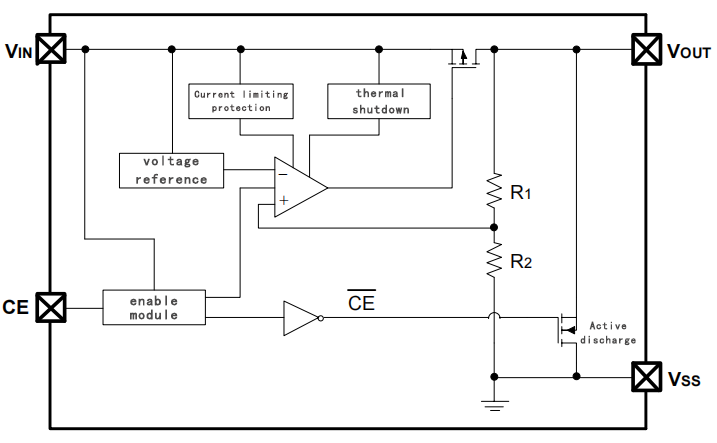
figure 1
Figure 1 is a functional schematic diagram of ICW2231, its basic circuit consists of a series adjustment tube, a sampling resistor, and a comparison amplifier.
Its basic working principle: when powered on, the enable pin is at a high level, the circuit starts, the constant current source circuit provides bias, the reference source voltage is quickly established, the output rises with the input, and when the output is about to reach the specified value, the feedback The output feedback voltage obtained by the network is also close to the reference voltage value. At this time, the error amplifier amplifies the small error signal between the output feedback voltage and the reference voltage, and then amplifies it to the output through the adjustment tube, thereby forming a negative feedback and ensuring the output voltage. It is stable at the specified value. Similarly, if the input voltage changes or the output current changes, this closed-loop loop will keep the output voltage unchanged, namely: Vout=(R1+R2)/R2 *Vref.
LDO related parameters
(1) Output Voltage
The output voltage is the most important parameter of a low dropout linear regulator, and it is also the first parameter that should be considered by electronic equipment designers when choosing a regulator. Low dropout linear regulators are available in fixed output voltage and adjustable output voltage types. The fixed output voltage regulator is more convenient to use, and since the output voltage is precisely adjusted by the manufacturer, the regulator has high precision. However, the set output voltage values are all common voltage values, which cannot meet all application requirements, but the change in the value of external components will affect the stability accuracy.
(2) Maximum Output Current
The power of the electrical equipment is different, and the maximum current required by the voltage stabilizer is also different. In general, regulators with higher output currents cost more. In order to reduce the cost, in the power supply system composed of multiple voltage stabilizers, the appropriate voltage stabilizer should be selected according to the current value required by each part.
(3) Input and output voltage difference (Dropout Voltage)
The input and output voltage difference is the most important parameter of the low dropout linear regulator. Under the condition that the output voltage is guaranteed to be stable, the lower the voltage dropout, the better the performance of the linear regulator. For example, a 5.0V low dropout linear regulator can stabilize the output voltage at 5.0V as long as the input voltage is 5.5V.
(4) Ground PIN Current
The grounding circuit IGND refers to the working current of the regulator provided by the input power supply when the output current of the series regulator is zero. This current is sometimes called quiescent current, but when a PNP transistor is used as a series pass element, this customary name is incorrect. Typically ideal low dropout voltage regulators have very little ground current.
(5) Load Regulation
The load regulation rate can be defined by the pressure difference between the red line and the blue line in Figure 2. The smaller the pressure difference, the smaller the load regulation rate of the LDO, indicating that the LDO has a stronger ability to suppress load interference.
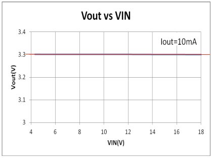
figure 2
(6) Linear adjustment rate (Line Regulation)
The linear adjustment rate can be defined by the voltage difference between the red line and the blue line in Figure 3. The smaller the voltage difference, the smaller the linear adjustment rate of the LDO, and the smaller the influence of the input voltage change on the output voltage, indicating that the better the performance of the LDO. it is good.

image 3
PCB Design for LDO Application
Key points of PCB board design: To obtain a stable and low-noise voltage regulator circuit or system, the layout structure of the PCB board should be carefully arranged. All devices must be close to the LDO. The PCB board can be divided into several pieces by function, as shown in Figure 4. .
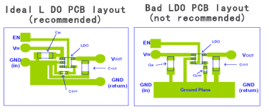
Figure 4
(1) Keep the path between the input voltage Vin and the output voltage Vout, and the grounding of the input capacitor Cin and the output capacitor Cout should be short to reduce noise and interference;
(2) The sampling resistors R1, R2 and the feedback capacitor CFB must be kept close to the FB feedback pin of the chip to prevent noise;
(3) The large area is directly connected to the GND pin of the chip and the negative end of the input capacitor Cin and the output capacitor Cout.
Finally, I will share with you the matters needing attention in the design of LDO (low dropout linear regulator):
(1) LDO maximum output current
Choose according to the 2/3 principle, that is, 3/2 times the total current consumption of the circuit. If the total current consumption of the circuit is 50 mA, then the maximum output current of the LDO is 75 mA.
(2) Package heat dissipation and power consumption
Power consumption = (input voltage - output voltage) * working current, choose the LDO package according to the 1/2 principle, if it cannot be achieved, the heat dissipation surface should be increased on the PCB, and the heat sink can be installed if the power consumption is large.
(3) Pay attention to pressure drop
Voltage drop = the voltage difference between the input voltage and the output voltage. The voltage drop meets the LDO specification to stabilize the output, otherwise the output does not meet the requirements. For example, an LDO with a voltage drop of 2V, if you want an output voltage of 5V, the input voltage needs to be 7V.
(4) Quiescent current
The quiescent current refers to the current that the LDO itself needs to consume. Especially for battery-powered products, LDOs with lower quiescent currents need to be selected to increase the standby time of the products.
(5) Filter capacitor
Refer to the requirements of the LDO specification, choose a suitable capacitor, and choose a capacitor with too small capacity, the output voltage may be unstable or the ripple is relatively large. If the input power ripple itself is relatively large, it is recommended to use larger capacity capacitors for the input and output terminals; the withstand voltage value of the capacitor also needs to be paid attention to, and the principle of 2 times is generally used for selection. If the input voltage is 24V, it is best to choose a capacitor with a withstand voltage of 50V. If the withstand voltage value is not 2 times or less than 1.5 times. Otherwise designed products are unreliable.
More News
What is LED driver power supply?
2021-09-15